Stock: Rise on Zen 6 Buzz and Game-Changing “Sea of Wires” Interconnect")
TLDR
- AMD’s Zen 6 interconnect slashes latency, boosts power and bandwidth.
- New “sea of wires” design unifies chiplets for faster, cooler performance.
- AMD Zen 6 CPUs set to scale better with efficient parallel interconnects.
- Strix Halo showcases AMD’s next-gen packaging and chiplet breakthroughs.
- Zen 6 interconnect redefines AMD’s edge in gaming, AI, and data centers.
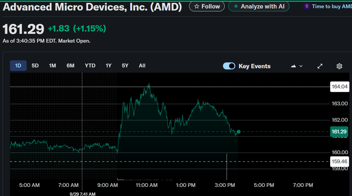
AMD stock climbed steadily on Monday, gaining 1.15% by mid-afternoon. The stock peaked near $164.04 before settling at $161.29.
Advanced Micro Devices, Inc. (AMD)
This upward movement reflected growing excitement around AMD’s upcoming Zen 6 CPU architecture. Much of the attention focuses on AMD’s new interconnect technology, which is already featured in its latest Ryzen AI MAX 300 series chips. This upgrade replaces traditional SERDES-based links with a denser, parallel “sea of wires” design. The approach significantly reduces latency, increases bandwidth, and improves power efficiency.
This design enables AMD to integrate its chiplets more closely, allowing them to behave more like unified silicon blocks. That gives upcoming Ryzen and EPYC CPUs an edge in performance across desktop, mobile, and data center platforms. Market watchers credit this innovation as a key driver behind the day’s price action.
Zen 6 prepares to shift AMD’s CPU architecture
AMD is transitioning from its current SERDES-based interconnect to a new chiplet design. The change relies on parallel wire routing supported by advanced packaging methods like TSMC’s InFO-oS. This structure eliminates traditional bottlenecks, allowing data to move faster with reduced power cost.

The redesigned interconnect lowers power usage by as much as 90% during data transfers between CPU and I/O dies. It also removes the need for repeated serialization and deserialization. That results in fewer delays and improves bandwidth per watt.
Zen 6 chips will benefit from better scalability and more efficient memory communication. By reducing memory latency, AMD improves gaming and high-performance computing workloads. These architectural changes aim to make AMD CPUs more competitive and responsive.
Strix Halo hints at what’s next for Ryzen and EPYC
AMD has already deployed the new interconnect in its Ryzen AI MAX 300 series, also known as Strix Halo. Engineers confirmed early sightings of the new design in photos, which showed missing SERDES blocks and dense pad arrays. These signs signal AMD’s shift toward a wider, fan-out based layout.
High Yield, a technical analyst on YouTube, documented these changes through hands-on testing with ASUS hardware. The interconnect aligns with AMD’s long-term packaging roadmap. It allows core chip components to sit closer together and share data more efficiently.
The results promise faster communication between CPU chiplets, memory controllers, and accelerators. Though the design introduces manufacturing complexity, AMD appears ready to scale it with Zen 6. If successful, it will redefine how AMD CPUs compete in performance-per-watt and latency-sensitive tasks.
Packaging evolution powers AMD’s CPU ambitions
Switching to a “sea of wires” layout introduces challenges in thermal handling and signal integrity. However, AMD has paired this strategy with co-designed packaging methods to ensure reliability. This includes multi-layer routing techniques under each die.
By freeing up space previously occupied by bulky SERDES blocks, AMD gains increased layout flexibility. That flexibility supports denser configurations and shorter communication paths. This setup is vital for high-bandwidth tasks and low-latency execution in modern computing environments.
Zen 6’s interconnect strategy will also help AMD scale core counts more efficiently. The bandwidth increases simply by adding more lanes, while power consumption remains under control. This gives AMD a foundation to improve both mobile and server-class performance in its upcoming chips.
Get 3 Free Stock Ebooks
Discover top-performing stocks in AI, Crypto, and Technology with expert analysis.
- Top 10 AI Stocks - Leading AI companies
- Top 10 Crypto Stocks - Blockchain leaders
- Top 10 Tech Stocks - Tech giants