Stock Surges 9% on New Chip Packaging Facility Plans")
Key Takeaways
- Shares of Samsung Electronics surged nearly 9% following reports the tech giant is exploring construction of a state-of-the-art chip packaging facility in Gwangju, South Korea.
- An official announcement regarding the investment could come during a June 29 summit between South Korean President Lee Jae Myung and top executives from major corporations.
- The proposed facility would bolster Samsung’s capabilities in advanced semiconductor packaging, a critical segment of the AI chip ecosystem.
- The company is competing intensely with SK Hynix in high-bandwidth memory (HBM) production, supplying processors to Nvidia, AMD, and Google.
- Samsung recently began distributing samples of its newest 12-layer HBM4E memory chip to potential clients.
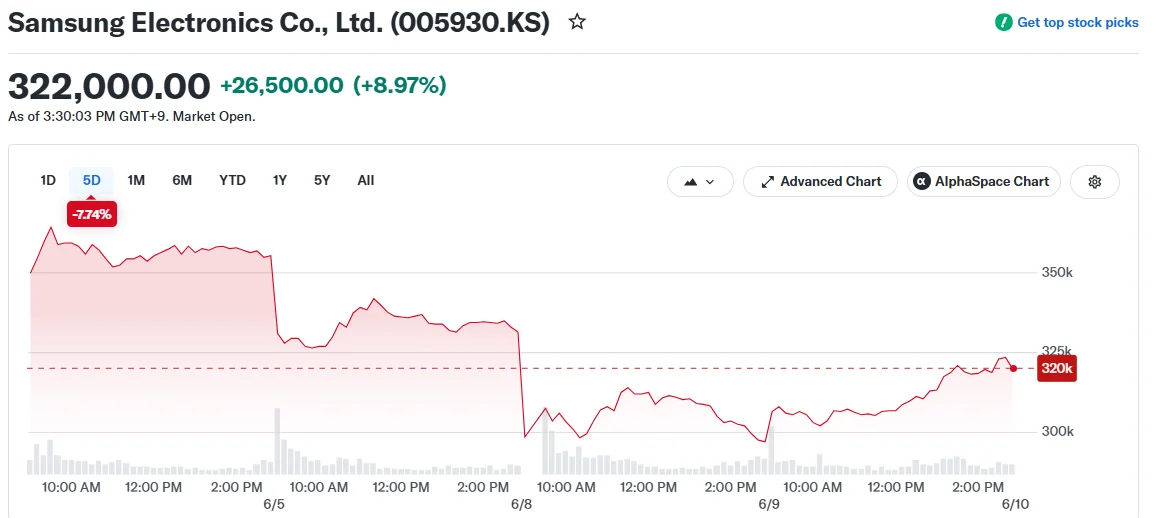
Shares of Samsung Electronics (005930) experienced a sharp rally on Tuesday, climbing nearly 9% after the Korea Economic Daily published a report indicating the semiconductor manufacturer is evaluating plans to construct an advanced packaging facility in Gwangju, located in southwestern South Korea.
According to the publication, which cited sources familiar with the matter, Samsung may unveil this investment strategy during a high-profile June 29 meeting at the presidential office. The meeting will bring together President Lee Jae Myung and chief executives from South Korea’s largest business groups.
Samsung Electronics Chairman Jay Y. Lee is anticipated to participate in the summit, alongside SK Group Chairman Chey Tae-won. The event is focused on discussing a “major shift in growth strategy” for the nation’s corporate landscape.
Samsung has not provided official comments on the media report. Representatives from the presidential office stated that investment choices remain within the purview of individual companies.
The Strategic Importance of Advanced Packaging
Advanced semiconductor packaging has emerged as a crucial competitive arena within the chip industry. This technology enables manufacturers to vertically stack and combine multiple chips within a single unit, enhancing overall performance without exclusively depending on transistor miniaturization.

Demand has surged particularly for high-bandwidth memory solutions. HBM technology vertically stacks multiple DRAM chips and works in tandem with AI accelerators from manufacturers like Nvidia. These components are essential for powering AI server infrastructure.
Samsung provides memory solutions to leading AI companies including Nvidia, AMD, and Google — all of which are fueling substantial demand for advanced memory architectures deployed in AI-focused data centers.
The establishment of a new packaging facility in Gwangju would signal Samsung’s commitment to accelerating capital investments in anticipation of a chip industry recovery driven by artificial intelligence applications.
The Race Between Samsung and SK Hynix
Samsung has been actively working to narrow the competitive gap with SK Hynix, which currently dominates the HBM market. Interestingly, SK Hynix shares also posted strong gains on Tuesday, climbing more than 15%.
Last month, Samsung announced it had begun distributing sample units of its latest memory solution, the 12-layer HBM4E chip, to prospective customers. This represents an advancement over previous generations and demonstrates the company’s determination to maintain competitive positioning.
The upcoming June 29 summit between government and business leaders could provide the formal platform for Samsung to publicly outline its strategic roadmap.
Samsung has yet to officially confirm the Gwangju facility plans, and the Korea Economic Daily’s report is based on information from anonymous industry sources.
Get 3 Free Stock Ebooks
Discover top-performing stocks in AI, Crypto, and Technology with expert analysis.
- Top 10 AI Stocks - Leading AI companies
- Top 10 Crypto Stocks - Blockchain leaders
- Top 10 Tech Stocks - Tech giants