Key Takeaways
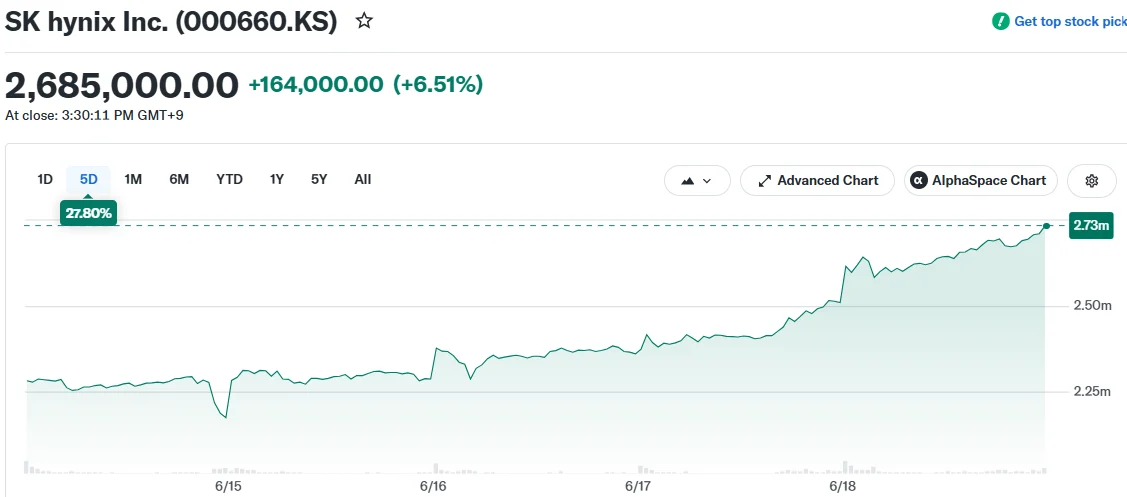
- SK Hynix shares climbed 6.51% following the announcement of HBM4E sample deliveries to key partners
- The advanced 12-layer memory chip achieves 16Gbps per pin speeds with over 20% improved power efficiency versus earlier versions
- Advanced MR-MUF manufacturing technology enables 48GB capacity with 17% enhanced thermal management
- SK Hynix maintains its position as Nvidia’s leading HBM provider amid competition from Samsung and Micron
- The chipmaker plans to collaborate with industry partners to accelerate mass production timelines
SK Hynix revealed on Thursday that it has delivered samples of its cutting-edge HBM4E memory chips to key industry partners, triggering a 6.51% surge in the South Korean semiconductor manufacturer’s shares on the Korea Exchange. The positive momentum extended to competitors, with Samsung’s stock advancing 4.62% and Micron gaining 2.20%.
The HBM4E represents a 12-layer, high-bandwidth memory solution designed specifically for artificial intelligence workloads. It achieves maximum data processing speeds of 16 gigabits per second per pin while providing over 20% superior power efficiency when compared to its HBM4 predecessor.
HBM memory chips serve as critical components within AI processors, including those manufactured by Nvidia. These chips manage the massive data volumes necessary for training and operating AI models. Without this specialized memory technology, the processors powering enterprise-scale AI applications cannot function effectively.
SK Hynix serves as Nvidia’s primary HBM supplier. While Samsung and Micron continue efforts to narrow the competitive gap, SK Hynix has maintained its market leadership across multiple technology generations — from HBM3 and HBM3E to the current HBM4 and HBM4E variants.
The company confirmed that the 12-stack HBM4E samples were shipped “on schedule,” attributing this achievement to its extensive expertise in HBM development and manufacturing capabilities.

Technical Innovations in HBM4E
The HBM4E reduces data transfer latency through enhanced interface architecture and design optimizations, while maintaining consistent performance in high-bandwidth computing environments. This capability proves essential for AI data centers operating continuous workloads at massive scale.
SK Hynix employs an innovative manufacturing technique known as Advanced MR-MUF — Mass Reflow Molded Underfill — which involves injecting liquid protective compounds between vertically stacked chips. This approach enables the company to achieve 48GB capacity within a 12-layer configuration while boosting thermal resistance by 17% compared to HBM4.
Enhanced thermal resistance translates to more dependable memory chip operation within high-performance computing platforms that produce significant heat output.
Path Toward Volume Manufacturing
Ahn Hyun, who serves as SK Hynix’s President and Chief Development Officer, stated the company has “laid the foundation to strengthen its AI leadership with HBM4E,” adding that it will collaborate with partners to bring the product to market while preserving its status as a “full-stack AI memory creator.”
The company declined to provide a precise mass production schedule, indicating only that it will “work closely with partners for mass production in a timely manner.”
Nvidia’s shares declined 1.33% on Thursday, though this movement was not directly connected to the SK Hynix announcement.
The HBM4E sample deliveries build upon SK Hynix’s proven history of supplying HBM3 and HBM3E to the marketplace — earlier generations that solidified its strategic partnership with Nvidia prior to the introduction of HBM4 technology.
Get 3 Free Stock Ebooks
Discover top-performing stocks in AI, Crypto, and Technology with expert analysis.
- Top 10 AI Stocks - Leading AI companies
- Top 10 Crypto Stocks - Blockchain leaders
- Top 10 Tech Stocks - Tech giants